Inside Qualcomm’s Snapdragon X2 Elite Efficiency Cores: Branch Prediction, Caches and Memory
Snapdragon X2 Elite’s 3.6 GHz efficiency cores pair a wide instruction cache and large shared L2 with narrower execution and memory pipelines.
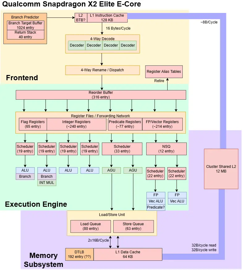
Qualcomm’s smaller Snapdragon X2 Elite cores are built to keep routine work moving with less emphasis on peak throughput. In the 18-core Snapdragon X2 Elite Extreme X2E96100, six “performance” cores sit alongside 12 “prime” cores. The smaller cores fill the role commonly assigned to efficiency cores: they can handle lightweight applications and background tasks without waking the larger cores, and add throughput when workloads use many threads.
Measurements of the efficiency core in the Asus Zenbook A16 UX3607OA show a design with deliberate trade-offs. It is a 4-wide, out-of-order core running at 3.6 GHz. That’s modest beside larger designs such as Intel’s Skymont, but width alone doesn’t determine how well a core handles everyday work. Qualcomm combines the narrower pipeline with branch prediction, backend resources and caches intended to keep it supplied with useful instructions.
The core also brings instruction set extensions that weren’t available on the Snapdragon X Elite. It supports SVE2 and SME, helping Qualcomm maintain extension support across the X2 Elite chip. Security-related extensions include pointer authentication and memory tagging (MTE).
Prediction and instruction delivery
Branch prediction matters for both speed and energy use: a wrong guess can leave execution resources waiting while the core fetches the right instructions. Qualcomm’s predictor covers the main requirements, though its design lacks some of the more elaborate features found in recent AMD, Arm and Intel cores.
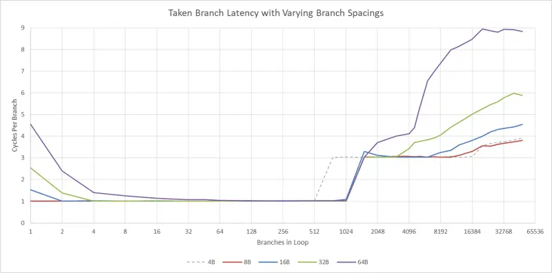
A 1,024-entry branch target buffer (BTB) can provide predictions for taken branches back-to-back. That is less peak throughput than the two taken branches per cycle supported by Intel and AMD’s larger cores and Arm’s Neoverse N2. Measurements also suggest that this BTB is separate from the L1 instruction cache. Unlike the earlier Oryon core in Snapdragon X Elite, its measured capacity doesn’t change with code footprint or branch spacing.
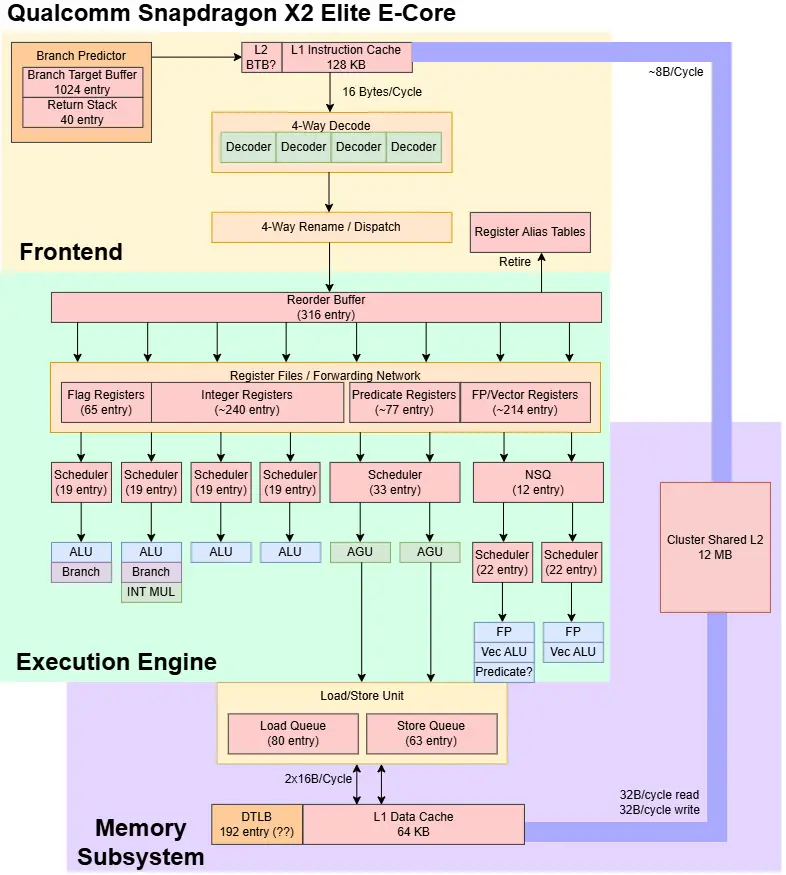
Once a test exceeds the BTB’s 1,024-entry capacity, throughput falls to one taken branch every three cycles. It drops again when the instruction footprint exceeds the 128 KB L1 instruction cache. One possible explanation is a second-level BTB linked to the instruction cache; another is that the core calculates direct branch destinations as instructions reach the decoder. Either approach would be simpler and take less area than a very large second-level BTB. The trade-off is that the predictor may not follow taken branches after an instruction-cache miss, making it harder to fetch ahead across large code footprints.
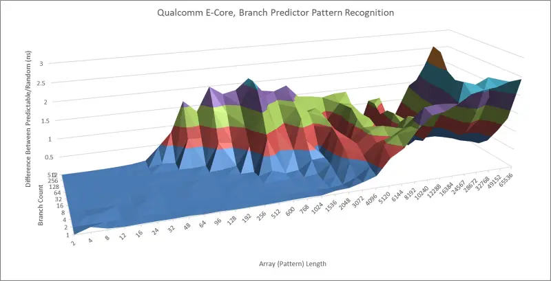
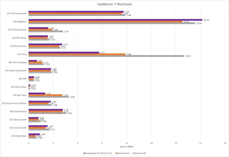
For predicting whether a branch is taken, Qualcomm’s core can learn long patterns and track many of them. It can follow roughly 16,000 patterns when 512 branches are active, or about 1,000 patterns for a single branch. Across Geekbench 7 workloads, its prediction accuracy is approximately on par with Arm’s Neoverse N2 and better than the Neoverse N1.
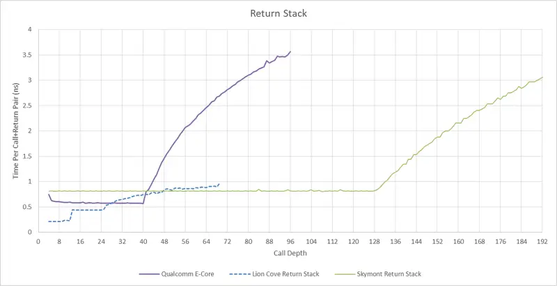
A 40-entry return stack handles function returns. It can sustain a call and return pair every two cycles, equivalent to one taken branch per cycle on average. That rate is faster than the return stack in AMD’s Zen 5 or Intel’s Skymont. Its capacity falls between Intel’s 128-entry stacks in Skymont and Crestmont and the 24-entry stack in Lion Cove.
Capacity alone doesn’t tell the whole story. Some designs, such as Lion Cove, appear to use another predictor when the return stack runs out, which can avoid a misprediction. In Qualcomm’s core and Intel’s Skymont, a return-stack underflow instead brings taken-branch latency to more than a dozen cycles, a sign that a misprediction has occurred. Qualcomm’s 40 entries offer more room before that penalty than Lion Cove’s stack, while stopping well short of Skymont’s capacity.
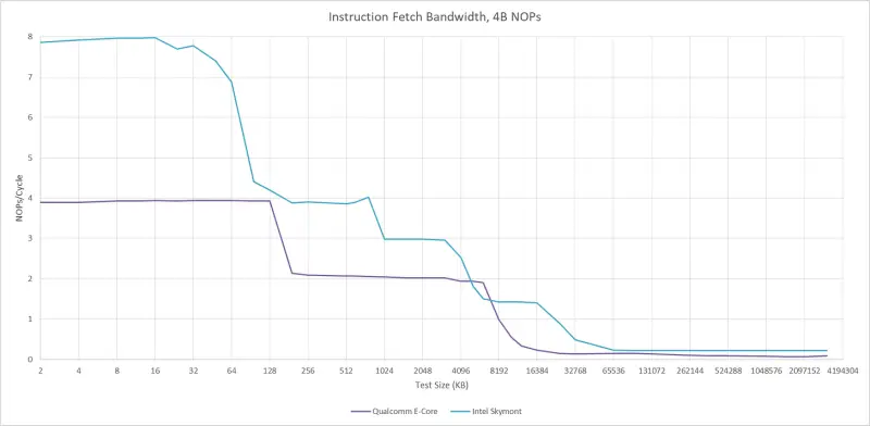
Qualcomm makes a similar capacity-versus-cost choice in instruction fetch. The 128 KB instruction cache is larger than the 32 KB or 64 KB caches common in contemporary designs, helping keep instruction delivery close to the core. When the working code spills into L2, frontend bandwidth falls to about two instructions per cycle. That’s usable, but below what Skymont can sustain from its shared L2. An L2 miss brings a much sharper drop in instruction bandwidth.
Execution resources and instruction handling
When instructions are decoded into micro-ops, the core allocates tracking resources so it can execute them out of order and retire them correctly. Qualcomm also uses this stage to remove some work before it reaches the execution units.
Register-to-register MOV instructions can be eliminated at up to two dependent moves per cycle. The register renamer does this by making two architectural registers refer to the same physical register, so an eliminated move takes no execution latency and needs no new physical register. That frees space in the core’s reordering resources.
There’s a wrinkle with chained moves. Long uninterrupted chains run at 1.38 moves per cycle, suggesting some moves are eliminated while others must use the execution units. Inserting NOPs so that a decode group contains no more than two moves raises throughput to two dependent moves per cycle. The more dependent moves packed into a single decode group, the less effectively the core eliminates them. Independent moves, which don’t depend on one another’s results, can run at four per cycle.
Small immediate additions can also be eliminated, but under tighter conditions. The limit is two per cycle, and the sum of immediates in eliminated additions must be 255 or less. For example, add x13, x13, 254 followed by add x13, x13, 1 can qualify; two add x13, x13, 128 instructions cannot. Intel’s Golden Cove handles this optimization at higher throughput and with larger immediates. Qualcomm doesn’t give MOV instructions that write zero a special case, either, so the core still allocates a physical register for the zero value.
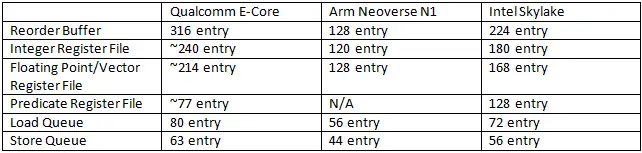
The backend’s reorder buffer and register files are sized more like AMD’s Zen 4 than older 4-wide designs such as Intel Skylake or Arm Neoverse N1. Memory-ordering queues are closer to Skylake’s sizing, though slightly larger.
Integer work gets four ALU ports, matching the core’s 4-wide design. A distributed scheduler feeds each port from a 19-entry queue. Three ports can handle flag-setting operations such as SUBS and CMP; one can execute integer multiplication with three-cycle latency. Two ports can resolve branches, but that rate depends on the branches being not taken. Taken branches are limited by the predictor’s throughput.
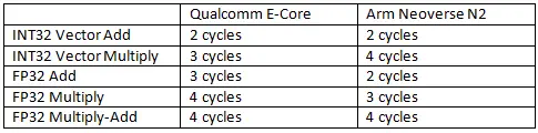
Floating-point and vector work has two execution ports. Both handle common floating-point and integer vector operations, along with cryptographic operations such as aese. Their latencies are typical for a modern core. SVE runs at a 128-bit vector length, so its contribution comes from additional instructions and predicate support rather than wider vector computation.
One floating-point and vector port can execute comparisons that write a predicate register, such as cmpeq. Predicate operations that don’t touch vector registers, including SVE’s while instructions, can use an integer port and preserve vector execution capacity. The core issues at most one while* instruction per cycle, suggesting that perhaps only one integer port can write to the predicate register file. SVE also supplies scatter and gather operations for non-contiguous memory accesses.
Memory access, translation and cache behavior
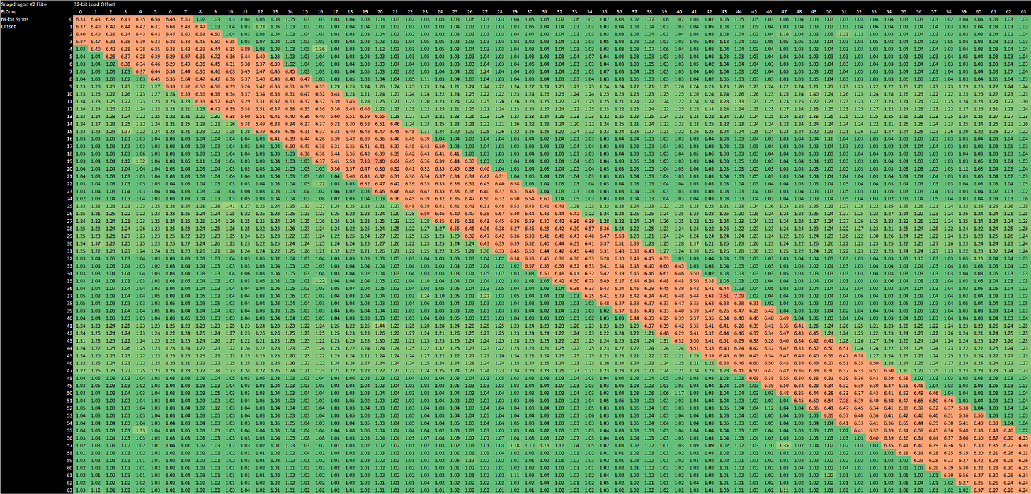
Two memory pipelines can each handle loads or stores. When an older store overlaps a later load, forwarding the stored data takes six to seven cycles, regardless of the load’s alignment within the store. The core avoids an extra failure penalty for partial overlaps, although it doesn’t offer the particularly fast exact-address match seen in Skymont.
Address translation relies on large translation lookaside buffers (TLBs), which cache virtual-to-physical address mappings. Qualcomm’s published figures give the larger X2 Elite cores a 224-entry, 7-way set-associative L1 data TLB (DTLB), backed by an 8K-entry L2 TLB. The company hasn’t specified the efficiency core’s capacities. Performance-counter measurements suggest it has large TLBs as well.
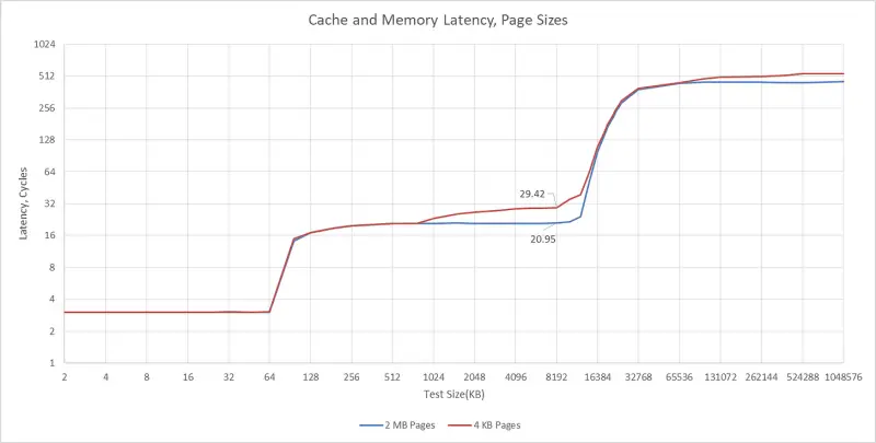
In those measurements, L1 DTLB misses rise when test sizes exceed 768 KB, consistent with a 192-entry L1 DTLB. L2 TLB misses begin beyond 32 MB, consistent with 8K entries. An L2 TLB lookup takes more than eight cycles, based on latency comparisons using 4 KB and 2 MB pages.
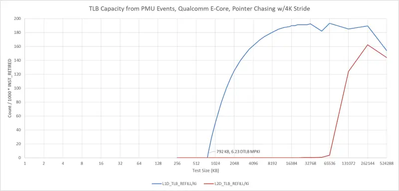
The TLBs support 4 KB and 64 KB pages, but not 16 KB pages. Windows uses 4 KB pages; Linux generally does too, though Ubuntu offers a kernel version that uses 64 KB pages. That range of support matters when matching a system’s memory-management setup to the core.
A 64 KB L1 data cache (L1D) returns a load in three cycles, or four cycles for indexed addressing. That combines more capacity with lower latency than many current cores, which use 32 KB or 64 KB L1D caches and often start at four cycles.
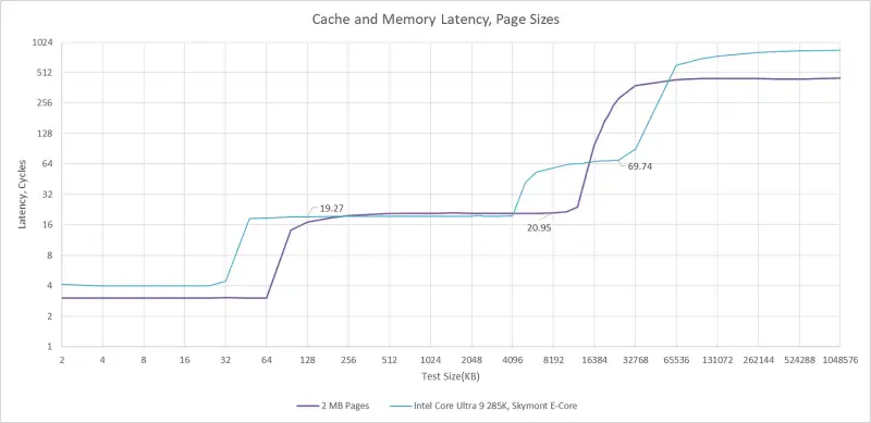
After an L1D miss, data comes from a shared L2 cache; Qualcomm doesn’t put a private mid-level cache between each core and L2. This resembles Apple’s M1 approach. L2 latency is 21 cycles, two cycles more than Skymont’s 4 MB shared L2. Skymont’s higher clock gives it lower absolute latency, but Qualcomm’s result is quick for the capacity provided.
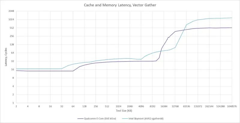
Gather operations show the cost of accessing scattered data. They process roughly one element per cycle, with latency just under 4 ns, or 14 cycles. There’s no measured sign of the combined-gather behavior described for Fujitsu’s A64FX and Monaka cores, where two elements from the same 64-byte or 128-byte block can be handled in one flow. For comparison, Skymont gathers take 3.7 ns, or 17 cycles, on an L1D hit. High gather latency is common enough that code using irregular data layouts shouldn’t assume vector instructions will make those accesses cheap.
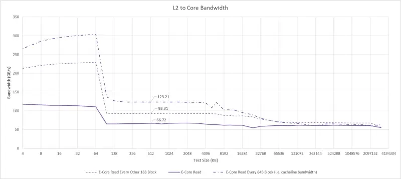
L1D bandwidth tops out at 32 bytes per cycle, in line with the 128-bit vector width and two memory pipelines. A linear read delivers a little over 16 bytes per cycle for data sizes that fit in L2, with no measured drop when the array reaches DRAM. The L2 itself can provide more than 32 bytes per cycle to a core, beyond what the execution pipes can use.
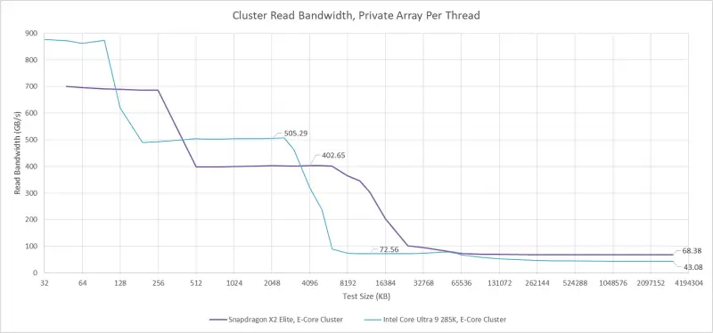
That higher L2 rate can be estimated by touching only part of each 64-byte cache line. An L1D miss still fetches the full line, whether the core uses all of it or only its first 128 bits. Under that measurement, the shared L2 delivers just over 400 GB/s to the six efficiency cores it serves. Per-core L2 bandwidth remains about 18 bytes per core cycle under load. Counting full cache lines touched suggests raw L2 bandwidth can exceed 500 GB/s, even though the cores can’t consume all of it. Skymont has smaller cluster-level caches but more cache bandwidth per core to feed its higher-throughput design.
A smaller core with a clear job
The 3.6 GHz, 4-wide efficiency core looks conservative beside Qualcomm’s own prime cores, which are 9-wide and run at 5 GHz, or Intel’s 8-wide, 4.6 GHz Skymont. But those larger cores target higher throughput. Qualcomm appears to have shaped this cluster around lightweight applications and background work, where keeping power consumption down can matter more than maximizing multi-thread throughput.
A narrower core is easier to feed and build. Wider designs need more complex renaming, instruction queues and decoders; when pipeline slots sit unused, much of that hardware does no useful work. At the other end, a core that is too narrow can make its width a frequent bottleneck. Intel kept 4-wide cores from Core 2 in 2006 through Skylake in 2015, a span that illustrates the lasting appeal of this design point.
My read is that Qualcomm’s “performance” label obscures the cluster’s practical role. These cores have capable prediction, sizable instruction and data caches, and substantial TLB capacity, but their execution width and memory bandwidth are restrained. They’re best understood as efficiency cores whose resources are tuned to keep background and less time-sensitive work moving without calling on the chip’s fastest cores.
 Choosing Single, Double, Welded Flap and Repair Keder for Fabrication
 Houston Engineering Team Builds a Welcoming Golf Tournament at East River 9
 MIG Transfer Modes: Choosing Between Short Circuit, Spray and Pulse