Semiconductor AI Shifts the Efficiency Challenge from Chips to Fabs and Supply Chains
AI is increasing silicon demand while changing how manufacturers use energy, analyze production data and coordinate across complex supply chains.
AI is pushing semiconductor manufacturing toward a three-part efficiency test: get more compute from each megawatt, more useful insight from each unit of manufacturing data, and more coordinated work from a supply chain spread across companies and countries. That shift matters beyond the current rise in chip demand. It changes how products are designed, tested and made—and how information moves between the organizations involved.
John Kibarian, chief executive of PDF Solutions, set out this view in a keynote at the company’s CONNECT event on October 15, 2026. He described a platform strategy built around three established areas: accelerating yield ramps for new technologies, applying current information technology to manufacturing data, and connecting manufacturing operations across the supply chain. PDF Solutions strengthened the last area with its 2025 acquisition of secureWISE.
The immediate constraint, Kibarian argued, is capacity already in place. A manufacturing executive told suppliers that no additional tools were available beyond those already promised. To meet demand, the company would have to get more production from its installed equipment. That pressure frames three linked challenges: energy efficiency in AI data centers, data and compute efficiency in manufacturing analysis, and coordination across increasingly distributed supply chains.
More AI capacity means more pressure on fabs
McKinsey & Company’s base case, as cited in the keynote, puts semiconductor device revenue at $975 billion in 2025 and about $2.3 trillion in 2030. That is an 83.5% increase in volume, with data centers and servers contributing 58% of the growth. The keynote puts that segment’s annual growth rate at 29%.
The implications for manufacturing capacity are substantial. Installed AI data center capacity of 45–60 GW in 2026 is projected to reach 100–160 GW by 2030. Using an estimate of 150,000–200,000 wafers per gigawatt, with half allocated to high-bandwidth memory (HBM), the keynote calculates demand for an additional 9.6–17.5 million wafers. At 50,000 wafer starts per month per fab, that would mean 16–29 new fabs.
That fab count may understate the challenge at the leading edge. The keynote notes that a modern leading-edge logic fab runs closer to 20,000 wafer starts per month, rather than 50,000. At that scale, the number of facilities needed could double. The figures depend on the stated capacity assumptions, but the underlying point is clear: expanding floor space and equipment is only one part of meeting demand.
Building out power-hungry data centers makes efficiency a design constraint, too. Kibarian cited projections of $3.9 trillion in AI revenue in 2030 and margins of roughly $30 million per megawatt. Those figures can make the buildout look chiefly like a capital problem. For fab operators, however, the harder task is extracting more compute from each data center and each unit of installed manufacturing capacity.
That goal is changing who designs silicon and what they optimize. Kibarian said that PDF Solutions previously saw many new customers among Asian fabs and fabless companies. More recently, foundation model companies and hyperscalers have begun designing their own silicon, with energy efficiency as a primary metric. Workloads also matter: training can keep a chip operating near its design point, while a GPU running inference may spend more than 90% of its power on memory updates and idle time, according to the keynote.
The keynote also invoked Richard Feynman’s 1980s lectures on the fundamental limits of computing, describing the industry as having roughly a factor of a million of headroom by that measure. It’s a reminder that improvements can come from architecture and workload design as well as from adding more facilities.
Manufacturing must adapt to more products and richer tests
As fabless companies design and manufacture more of their own silicon, Kibarian said, their need for manufacturing software has grown. Much of the work now happens after wafers leave the front-end fab, across assembly, packaging, test and related operations.
Energy-efficient custom designs bring operational consequences: smaller production volumes spread across more products, rather than a few high-volume parts. New-product introduction testing also generates broader datasets and test programs that can contain millions of test items. Those requirements carry into production, where teams need to ramp yield quickly while handling more variation across products.
Integration methods add further process-control demands. Co-packaged optics and similar technologies put more than electrons into the production flow, requiring manufacturers to account for new materials and interfaces. These changes make design and manufacturing data more interdependent: teams need enough design context to locate defects and enough process information to determine what caused them.
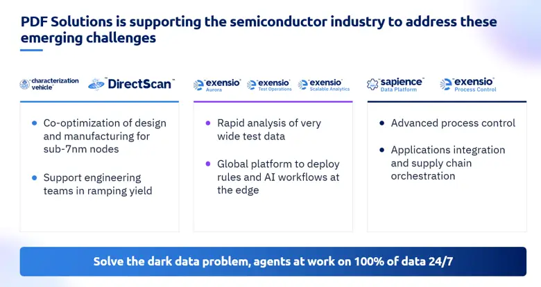
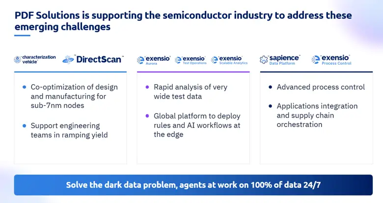
PDF Solutions positions several products around these needs. The company says Characterization Vehicle and DirectScan support design and manufacturing co-optimization at sub-7nm nodes, using design information to guide inspection, including e-beam approaches intended to find buried systematic defects in three-dimensional structures. Exensio Aurora, Exensio Test Operations and Exensio Scalable Analytics are aimed at analyzing wide test datasets and deploying rules and AI workflows closer to production equipment.
The company also describes a Python-first, natively parallel compute engine that shifts analysis from a client computer to a scalable back end. PDF Solutions claims it delivers 20–40 times the performance for the same hardware spend by using processor cores more efficiently. Sapience and Exensio Process Control extend the portfolio into process control, application integration and supply chain coordination.
Manufacturing AI needs private context
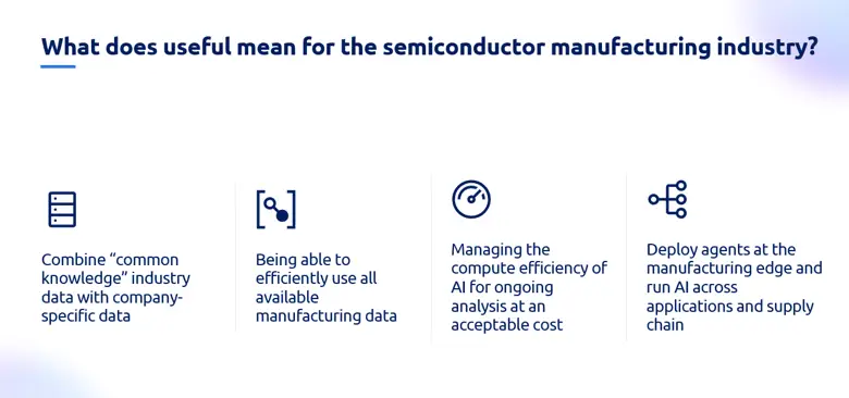
For manufacturing, an AI system is useful only if it can combine general semiconductor knowledge with a company’s own data and operating history. It must also use the available data efficiently, keep ongoing compute costs manageable and support software agents at the manufacturing edge and across supply chain applications.
General-purpose language models can already work with familiar concepts such as wafer maps, parametric test, bins, lots, statistical process control charts, etch-rate drift and failure mechanisms. They can suggest analytical methods, generate code and summarize unstructured information. Given a yield loss across several lots, a model may produce a reasonable first set of analyses.
The harder step is interpreting an ambiguous result. A less experienced engineer may see an unfamiliar signal, dismiss it as noise and conclude that the data shows nothing. A senior engineer may recognize a meaningful pattern because they know the product history and process context. That context includes company-specific intellectual property, historical baselines, recipes, design rules, test flows and bin definitions. It also takes substantial statistical computation and validation to establish whether an apparent signal is real.
Data volume compounds the problem. The keynote says leading fabless companies and large foundries can hold petabytes of data per site across more than 20 domains, with at least 100 file formats in each domain. A new 3D-IC can have 2–10 million test parameters during new-product introduction. Even mixed-signal companies with test programs of about 10,000 parameters may accumulate around 200 TB of analytics data.
At one foundry, the analysis task involves 2–3 trillion sort parameters across roughly 2,000 products each week, with more than 100,000 features per unit. The keynote says these organizations have more products than product and test engineers. That makes it difficult for engineers to know which data will matter before a yield problem appears; in post-mortems, Kibarian said, the relevant information is often already present.
PDF Solutions says Exensio Aurora draws on 30 years of semiconductor manufacturing knowledge to supply context for AI analysis. The company cites petabytes of manufacturing data held on isolated customer cloud sites, more than 1,000 test chips taped out for process characterization over 15 years, and over 660,000 customer-built analytics templates and practices. It also describes a semiconductor ontology that aligns data from different sources. The company says customer data and the agents operating on it remain isolated between sites.
Run repeatable analysis as a workflow
The cost of repeated language-model calls is another limit. Kibarian described tokens as a fast-growing information technology expense and gave an example of a developer whose token allowance ran out at 2 p.m. A task estimated to take five hours by hand took five minutes once access was restored. The example shows the time saved, but also why a manufacturing team cannot assume that running a language model for every analysis will remain economical.
For a repeated analysis of a 100,000-row, 10-column sample, the keynote compares three approaches. Asking a language model to analyze the data each time uses 30,000 tokens and 30 Wh per analysis. Asking it to create the analytical workflow once uses 20,000 tokens and 20 Wh. Running that stored workflow on each new sample uses 0.02 Wh per run, with no further token use in the comparison.
Those figures are the keynote’s example, not a universal measurement for every workload. They illustrate the tradeoff: language models can help create an analysis, while conventional compute can repeat it at far lower energy cost. For a task that recurs, generating and storing the workflow can make the result more predictable and reduce dependence on repeated model calls.
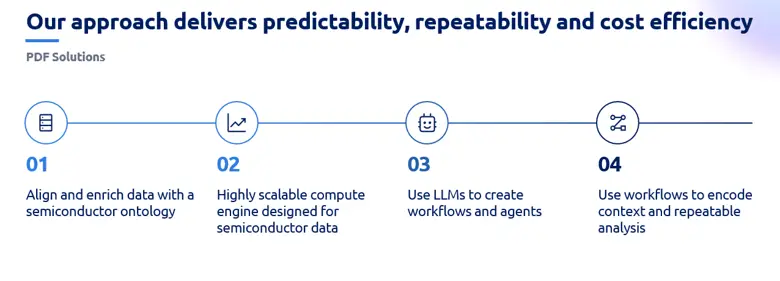
PDF Solutions’ approach uses Python as the language for creating these workflows. First, a semiconductor ontology aligns terms such as lots, wafers, bins, tests and tools. Then a compute engine designed for semiconductor datasets performs the analysis, avoiding the need to pull large datasets through application programming interfaces for a language model to process directly.
The model’s role is to generate a workflow or agent rather than to perform every calculation itself. Engineers can inspect the result as visual workflow blocks, run it, and, if it works, generalize and store it for reuse. That captures the analytical context in a form teams can review and repeat. The company says its architecture also keeps customer data separated from the language model, allowing customers to try models that do not run on site while keeping manufacturing data within their control.
Secure connections extend from fabs to suppliers
Hybrid packaging turns manufacturing into a multi-company execution problem. Wafer fabrication, die preparation, wafer bonding, die stacking, through-silicon vias and interconnects, advanced packaging, testing and metrology can each happen at a different facility, under a different company, and in a different country.
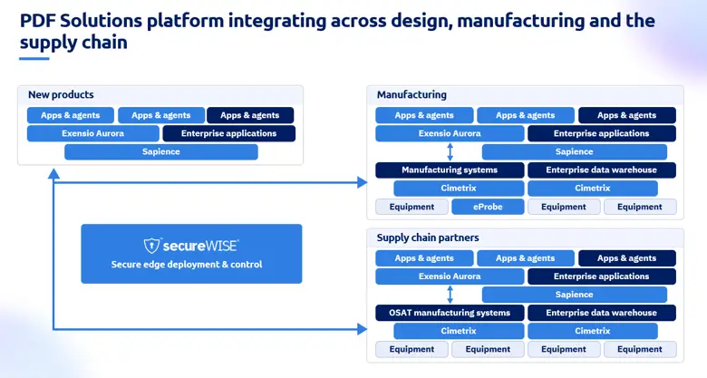
PDF Solutions acquired secureWISE to extend its work across these connections. Kibarian described it as a network linking fabs with equipment vendors, including deployment in 3nm fabs and the movement of exabytes of data between suppliers and factories. Some equipment vendors use the network to gather data across their installed equipment, develop improved algorithms and return software to tools.
The company describes control over data movement as a key feature. Traffic is encrypted twice, and packet contents are not shared. Factory teams decide what information leaves a facility and when, what data and algorithms return, what scanning applies to incoming material, and how activity is recorded. Those controls matter as more analysis and software updates move between organizations.
secureWISE was designed for human collaboration, but Kibarian said much of its traffic and associated revenue now comes from data leaving facilities and software or algorithms returning. In practice, that means software agents and AI systems increasingly participate in the same cross-company exchanges once handled mainly by people. The expected growth in agent activity raises the need for clear control over what each system can send and receive.
A shared platform for efficiency
PDF Solutions presents its platform as a way to connect the three efficiency problems. Data centers need more compute per megawatt; manufacturers need more useful analysis per token and per processor core; and supply chain partners need to exchange data and algorithms with appropriate control.
In the company’s architecture, Exensio Aurora and enterprise applications run on Sapience, with applications and agents layered on top. In fabs and outsourced semiconductor assembly and test (OSAT) facilities, Cimetrix connects equipment, including eProbe, to manufacturing systems and enterprise data warehouses. secureWISE provides the secure edge connection across sites, allowing data, rules, workflows and agents to move under the control of the organizations that own the data.
The practical test for this approach will be whether manufacturers can put more of their existing equipment, data and engineering knowledge to work as product variety and production complexity increase. The next efficiency gains may depend as much on repeatable analysis and controlled data exchange as on adding new silicon capacity.
 Choosing Single, Double, Welded Flap and Repair Keder for Fabrication
 Houston Engineering Team Builds a Welcoming Golf Tournament at East River 9
 MIG Transfer Modes: Choosing Between Short Circuit, Spray and Pulse