Acoustic Micro Imaging Reveals Hidden Defects in Advanced Packaging
High-frequency ultrasound maps package layers to find gaps and delamination, while newer scanning methods aim to raise wafer inspection throughput.
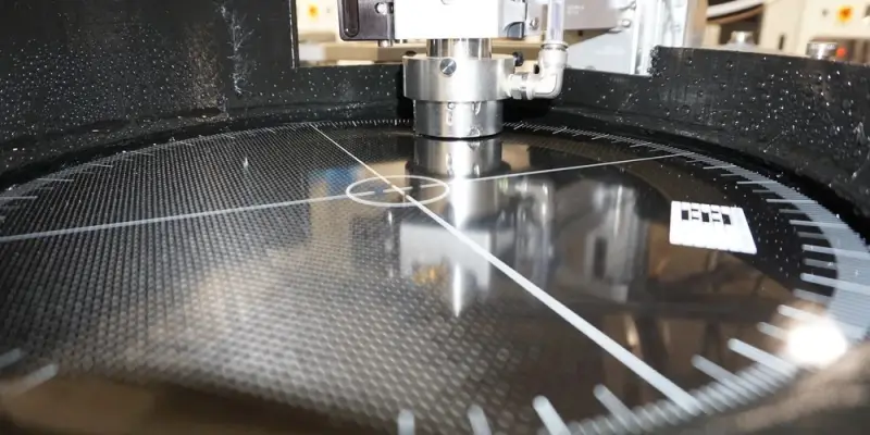
As advanced packages add layers, dies and tighter interfaces, hidden gaps and weak attachment layers can threaten device reliability. Acoustic micro imaging (AMI) gives engineers a non-destructive way to inspect those internal features with high-frequency ultrasound, producing layer-by-layer images that help identify defects before they become failures.
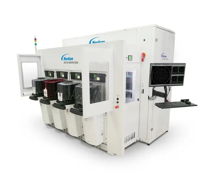
The method is useful when visual inspection cannot reach an internal interface. Delamination and air gaps can compromise electrical or mechanical performance, while thinning or unevenness in solder attach and thermal interface material (TIM) layers can point to problems in the build process. Those findings make AMI relevant both to production inspection and to process development.
Turning ultrasound echoes into layer images
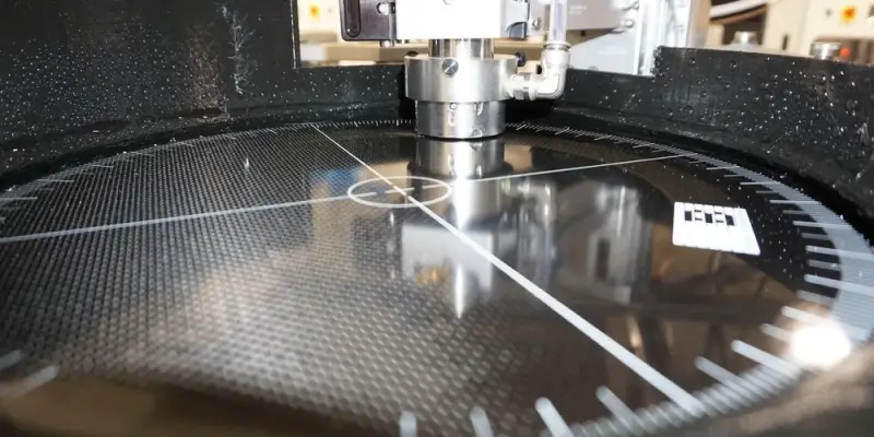
An AMI system uses a transducer to convert an electrical pulse into a high-frequency mechanical wave. The transducer scans across the sample, and the system collects measurements at locations across its surface. Since ultrasound does not travel through air, an air gap changes the signal at an interface; that contrast lets the system show gaps and delaminations that may be difficult to observe by other means.
Frequency selection matters. Transducers operate at specific frequencies, and the appropriate choice depends on the sample being inspected. The scan produces multiple images, which AMI software analyzes for features associated with defects. Inspectors can then assess the results against the acceptance criteria for the part. The source material does not specify universal defect thresholds, so those criteria depend on the application and inspection process.
Defects can take more than one form. A clear air gap is a direct indication of a discontinuity between layers. A thin attach layer presents a different concern: under stress, it may be more susceptible to delamination. Uneven solder or TIM thickness can also signal variation in assembly or material application. The practical value of the image is therefore not limited to finding an obvious void; it can help flag interface conditions that merit closer process review.
Where destructive checks and X-ray fit
A non-destructive scan does not make destructive testing unnecessary in every case. During research and development, a team may need to establish that an AMI indication corresponds to a real void or delamination. Destructive analysis can provide that proof of concept before the inspection software is adopted in a production workflow. Capacitor inspection is one example: new capacitor suppliers may use destructive checks to confirm defects identified by AMI.
That distinction matters when building confidence in a new inspection method. AMI software can classify image features, but a process under development may still need physical confirmation that the classifications match the condition of the part. Once that relationship has been established, the method can be incorporated into inspection, subject to the company’s chosen criteria and operating procedure.
X-ray and ultrasound provide different views of a package. AMI examines the sample layer by layer. Transmission scanning uses a sending and receiving transducer on opposite sides of the sample, and, like X-ray, produces a composite image. A composite view can be useful for spherical features such as ball grid arrays, while AMI’s layer-resolved images can help locate which interface contains a suspect feature. The technologies are complementary, and some applications may benefit from both.
Adapting inspection to denser packages
AMI systems face a moving target as package structures grow more complex. Software developed to inspect a single flip chip may need to handle multi-die stacks, where the number and arrangement of interfaces add to the interpretation challenge. Higher resolution and faster inspection are also competing demands: capturing more detail can require more data, while production lines need useful results at pace.
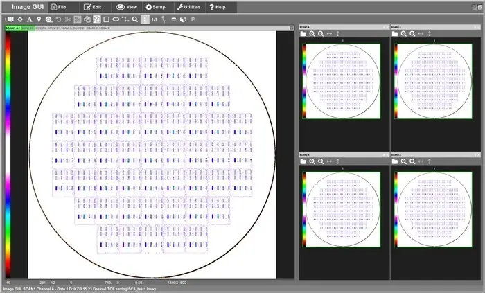
Machine learning is being applied to a specific classification problem. Some wafers contain via patterns that can look like delamination in an acoustic image. Historically, people have distinguished those patterns during review. The described software approach uses machine learning to recognize via patterns and leave them out of the defect count. That can reduce false indications from known structures, though the source provides no performance figures or test conditions for the capability.
Scanning mechanics also affect throughput. A conventional acoustic microscope moves its transducer in a raster, collecting data across a grid of XY points. At the end of each line, it must slow down and reverse direction. Some systems skip lines and interpolate between measured points, or combine scans from multiple transducers by stitching images together; those approaches bring trade-offs in data coverage or image quality.
Nordson Test & Inspection developed the automated SpinSAM system to address throughput requirements. The company says it can inspect four 300mm wafers at a time. Rather than following a stop-and-turn raster path, SpinSAM rotates the wafer so scanning can continue as the transducer moves. The manufacturer describes this as a way to scan pixels faster without the distortion associated with stitching images.
For engineering teams, the choice of inspection method depends on the defect of interest, package geometry and required production rate. AMI’s strongest contribution is its ability to expose internal interfaces without sectioning a part, while destructive checks can validate findings during process development and X-ray can supply a useful composite view. As packages move toward stacked dies and more intricate layer structures, inspection software and scan motion will determine how well that detail can be captured at production speed.
 Choosing Single, Double, Welded Flap and Repair Keder for Fabrication
 Houston Engineering Team Builds a Welcoming Golf Tournament at East River 9
 MIG Transfer Modes: Choosing Between Short Circuit, Spray and Pulse